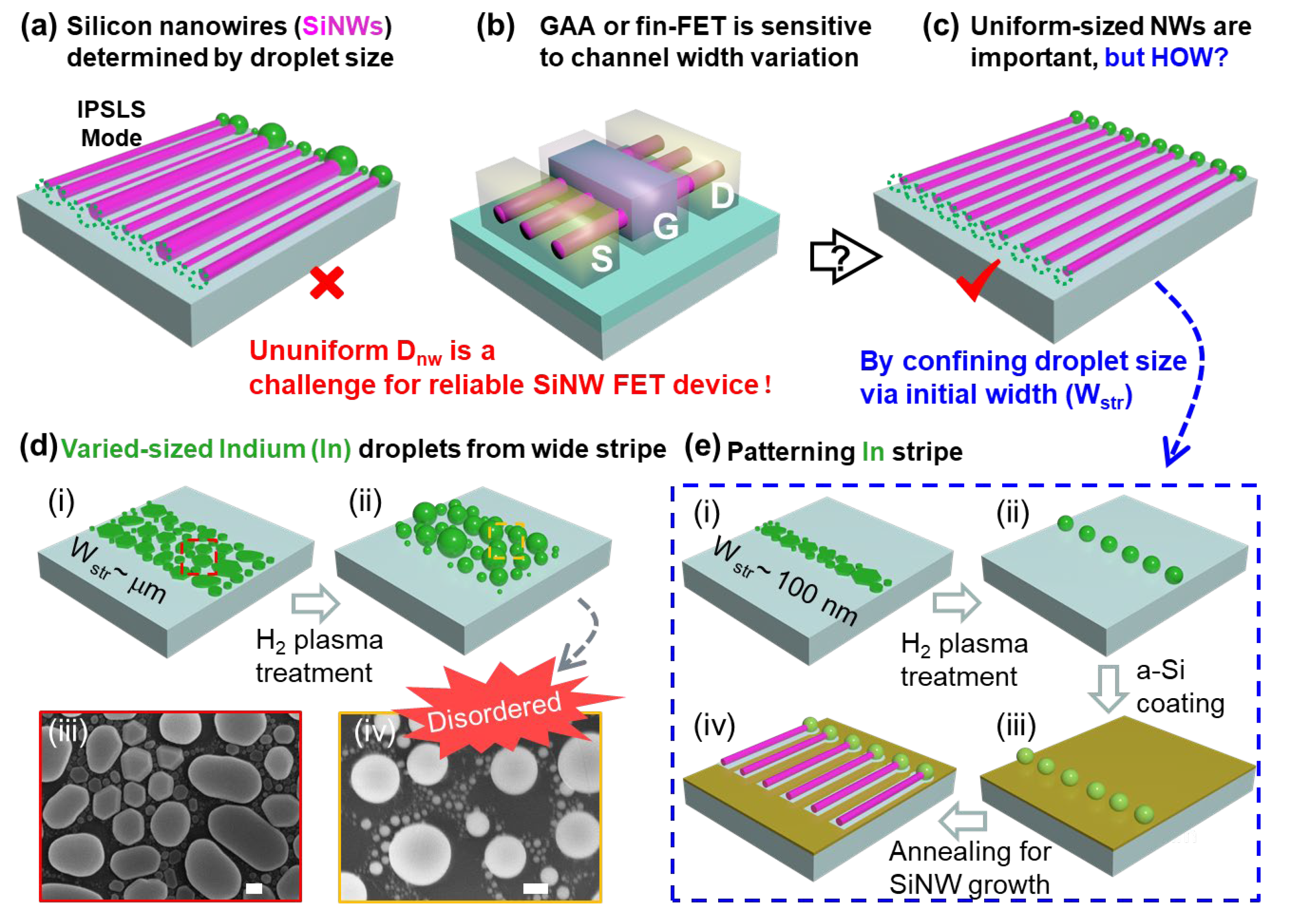
Obtaining Uniform Dopant Distributions in VLS-Grown Si Nanowires
4.9 (689) · $ 21.99 · In stock


Carrier Dynamics in Si Nanowires Fabricated by Metal-Assisted

TEM images of GDNWs. (a to e) GDNWs without washing with HCl: (a), (b)

TEM for Characterization of Nanowires and Nanorods

Nanomaterials, Free Full-Text
Schematic diagrams illustrating the growth of ZnO nanorods
Quantifying charge carrier concentration in ZnO thin films by Scanning Kelvin Probe Microscopy

PDF] Spatially resolved correlation of active and total doping

a)-(c) SEM micrographs of undoped (0A) and Si-doped (11A,13A) GaAs

Doping of semiconductor nanowires

Cross-field optoelectronic modulation via inter-coupled ferroelectricity in 2D In2Se3

Formation and characterization of Group IV semiconductor nanowires - IOPscience

Growth of nanowire heterostructures and their optoelectronic and spintronic applications - ScienceDirect
Nanomaterials, Free Full-Text

Schematic illustration of NW doping procedure showing (a) Si NW